- 您现在的位置:买卖IC网 > Sheet目录364 > SST49LF016C-33-4C-EIE-T (Microchip Technology)IC FLASH SER LPC 16MBIT 40TSOP
�� �
�
�16� Mbit� LPC� Serial� Flash�
�A� Microchip� Technology� Company�
�SST49LF016C�
�Data� Sheet�
�Non-boundary-aligned� address:�
�The� SST49LF016C� accepts� multi-byte� transfers� for� both� Read� and� Write� operations.� The� device�
�address� space� is� divided� into� uniform� page� sizes� 2,� 4,� 16,� or� 128� bytes� wide,� according� to� the� MSIZE�
�value� (see� Table� 6).� The� host� issues� only� one� address� in� the� MADDR� field� of� the� Firmware� Memory�
�Cycle,� but� multiple� bytes� are� read� from� or� written� to� the� device.� For� this� reason� the� MADDR� address�
�should� be� page� boundary-aligned.� This� means� the� address� should� be� aligned� to� a� Word� boundary� (A� 0�
�=� 0)� for� a� 2-byte� transfer,� a� double� Word� boundary� (e.g.� A� 0� =� 0,� A� 1� =� 0)� for� a� 4-byte� transfer,� and� so� on.�
�If� the� address� supplied� by� the� host� is� not� page� boundary-aligned,� the� SST49LF016C� will� force� a�
�boundary� alignment,� starting� the� multi-byte� Read� or� Write� operation� from� the� lower� byte� of� the�
�addressed� page.�
�Multiple� Device� Selection�
�Multiple� LPC� serial� flash� devices� may� be� strapped� to� increase� memory� densities� in� a� system.� The� four�
�ID� pins,� ID[3:0],� allow� up� to� 16� devices� to� be� attached� to� the� same� bus� by� using� different� ID� strapping� in�
�a� system.� BIOS� support,� bus� loading,� or� the� attaching� bridge� may� limit� this� number.� The� boot� device�
�must� have� an� ID� of� 0000b� (determined� by� ID[3:0]);� subsequent� devices� use� incremental� numbering.�
�Equal� density� must� be� used� with� multiple� devices.�
�Multiple� Device� Selection� for� Firmware� Memory� Cycle�
�For� Firmware� Memory� Read/Write� cycles,� hardware� strapping� values� on� ID[3:0]� must� match� the� values�
�in� IDSEL� field.� The� SST49LF016C� will� compare� these� bits� with� ID[3:0]’s� strapping� values.� If� there� is� a�
�mismatch,� the� device� will� ignore� the� remainder� of� the� cycle.� See� Table� 7� for� Multiple� Device� Selection�
�Configuration.�
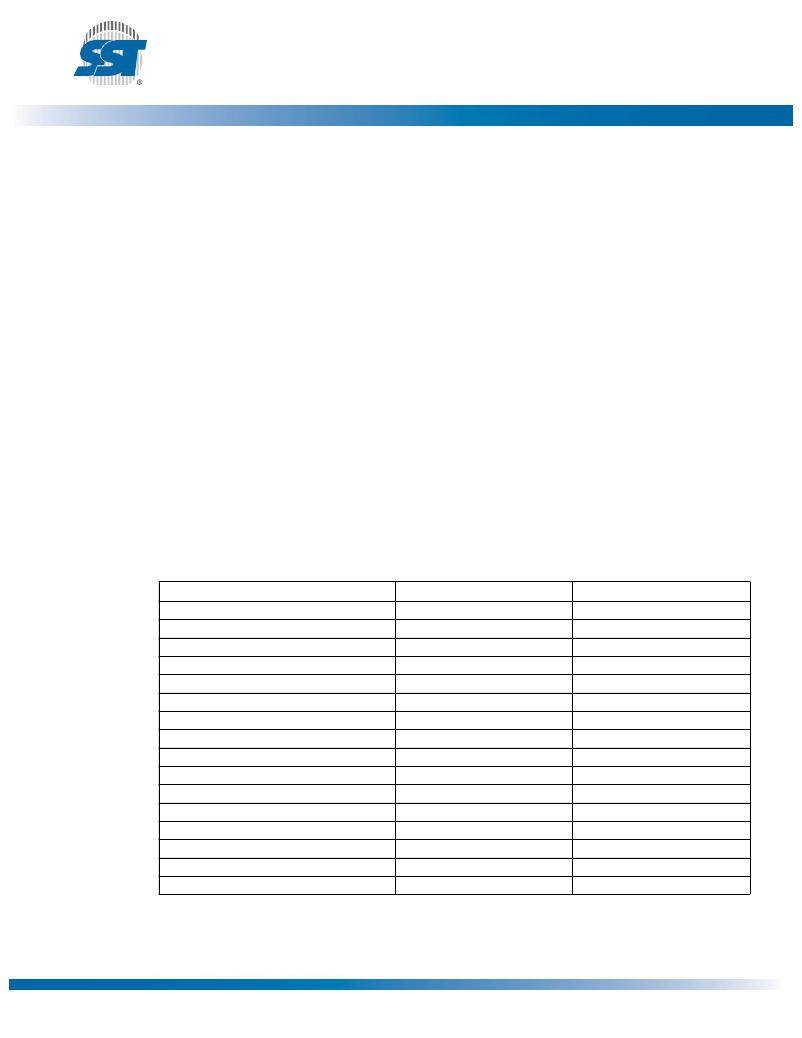
�Table� 7:� Firmware� Memory� Multiple� Device� Selection� Configuration�
�Device� #�
�0� (Boot� device)�
�1�
�2�
�3�
�4�
�5�
�6�
�7�
�8�
�9�
�10�
�11�
�12�
�13�
�14�
�15�
�ID[3:0]�
�0000�
�0001�
�0010�
�0011�
�0100�
�0101�
�0110�
�0111�
�1000�
�1001�
�1010�
�1011�
�1100�
�1101�
�1110�
�1111�
�IDSEL�
�0000�
�0001�
�0010�
�0011�
�0100�
�0101�
�0110�
�0111�
�1000�
�1001�
�1010�
�1011�
�1100�
�1101�
�1110�
�1111�
�T7.0� 25029�
�?2011� Silicon� Storage� Technology,� Inc.�
�15�
�DS25029A�
�06/11�
�发布紧急采购,3分钟左右您将得到回复。
相关PDF资料
SST49LF080A-33-4C-WHE-T
IC FLASH SER LPC 8MBIT 32TSOP
SST49LF160C-33-4C-NHE
IC FLASH SER LPC 16MBIT 32PLCC
ST40
DIAC 35-45V BILATERAL TRIG DO214
STRIKER
SURGE SUPPRESSR 120V 7OUT 6'CORD
SUPER-7
SURGE SUPPRESSOR 7 OUT 7' CORD
SUPER6TEL12
SURGE SUPPR 7OUT 12'CORD W/RJ11
SUPER6TEL
SURGE SUPPRESSOR 7OUT W/TEL
SUPER7COAX
SURGE SUPPRESSOR 7 OUT W/COAX
相关代理商/技术参数
SST49LF016C-33-4C-NHE
功能描述:闪存 16M (2Mx8) 33MHz 3.0-3.6V Commercial RoHS:否 制造商:ON Semiconductor 数据总线宽度:1 bit 存储类型:Flash 存储容量:2 MB 结构:256 K x 8 定时类型: 接口类型:SPI 访问时间: 电源电压-最大:3.6 V 电源电压-最小:2.3 V 最大工作电流:15 mA 工作温度:- 40 C to + 85 C 安装风格:SMD/SMT 封装 / 箱体: 封装:Reel
SST49LF016C-33-4C-NHE-T
功能描述:闪存 3.0 to 3.6V 16Mbit LPC Firmware 闪存 RoHS:否 制造商:ON Semiconductor 数据总线宽度:1 bit 存储类型:Flash 存储容量:2 MB 结构:256 K x 8 定时类型: 接口类型:SPI 访问时间: 电源电压-最大:3.6 V 电源电压-最小:2.3 V 最大工作电流:15 mA 工作温度:- 40 C to + 85 C 安装风格:SMD/SMT 封装 / 箱体: 封装:Reel
SST49LF016C-33-4C-WHE
功能描述:闪存 16M (2Mx8) 33MHz 3.0-3.6V Commercial RoHS:否 制造商:ON Semiconductor 数据总线宽度:1 bit 存储类型:Flash 存储容量:2 MB 结构:256 K x 8 定时类型: 接口类型:SPI 访问时间: 电源电压-最大:3.6 V 电源电压-最小:2.3 V 最大工作电流:15 mA 工作温度:- 40 C to + 85 C 安装风格:SMD/SMT 封装 / 箱体: 封装:Reel
SST49LF016C-33-4C-WHE_
制造商:Microchip Technology Inc 功能描述:
SST49LF016C-33-4C-WHE-T
功能描述:闪存 3.0 to 3.6V 16Mbit LPC Firmware 闪存 RoHS:否 制造商:ON Semiconductor 数据总线宽度:1 bit 存储类型:Flash 存储容量:2 MB 结构:256 K x 8 定时类型: 接口类型:SPI 访问时间: 电源电压-最大:3.6 V 电源电压-最小:2.3 V 最大工作电流:15 mA 工作温度:- 40 C to + 85 C 安装风格:SMD/SMT 封装 / 箱体: 封装:Reel
SST49LF016C-66-4C-NHE
制造商:SST 制造商全称:Silicon Storage Technology, Inc 功能描述:16 Mbit LPC Serial Flash
SST49LF016C-66-4C-WHE
制造商:SST 制造商全称:Silicon Storage Technology, Inc 功能描述:16 Mbit LPC Serial Flash
SST49LF020
制造商:SST 制造商全称:Silicon Storage Technology, Inc 功能描述:2 Megabit LPC Flash